Dive into the capabilities of XFdtd’s schematic editor and discover how it transforms schematic creation, analysis, and optimization in engineering.
XFdtd’s schematic editor is an integral tool for engineers and designers working in antenna design and analysis applications. As technology evolves, so does the complexity of designing and optimizing schematics in various applications. This guide provides an insightful look into the updated features of the schematic editor, highlighting its utility in creating efficient, optimized designs and integrating these with full-wave simulation results.

Key features of the schematic editor include:
- A user-friendly interface that simplifies the process of schematic creation
- Advanced analytical tools that allow for detailed performance assessments
- Optimization capabilities that automate the refinement of antenna designs
- Seamless integration with 3D electromagnetic simulations
- Comprehensive support for a wide range of antenna design scenarios
Creating and Analyzing Schematics
The process of creating a schematic using XFdtd involves the selection of an array of components, each with specific functions and characteristics. These components are carefully arranged according to a well-defined topology, tailored to the project's specific needs. The analysis phase in XF is straightforward yet impactful, concentrating on the interactions among various components within the schematic. This phase is crucial as it ensures all parts work harmoniously towards achieving the predefined design goals. These goals can range from enhancing system efficiency to achieving targeted S-parameters, which are critical metrics in many engineering projects. Through this process, XF helps engineers systematically organize and scrutinize each element of their design to ensure optimal performance and functionality.
Steps in the process include:
- Selection of components from a comprehensive toolbar tailored for matching network design
- Placement of these components in the schematic to simulate the physical layout
- Definition of connections between components to establish the flow of signals
- Configuration of different loading scenarios within the same schematic to test versatility
- Adjustment of parameters to cater to specific use cases and precise applications

Design Goals and Optimization
Establishing clear and precise design goals is fundamental in steering the optimization process effectively. The schematic editor empowers users to define specific target metrics that align with their project requirements. This is facilitated through a user-friendly, dynamic interface equipped with tuning sliders that allow for real-time adjustments and iterating. These sliders provide immediate visual feedback on changes, enabling users to understand the impact of their modifications instantly. Furthermore, the recent integration of an advanced optimization feature significantly bolsters the tool's capability to meet these design goals with greater precision and efficiency.

Key benefits:
- Real-time updates enable immediate feedback on any adjustments made.
- Iterative design improvements help in refining antenna performance progressively.
- Engineers can set specific design goals within the software.
- The system automatically adjusts component values to align with specified targets.
- This automated adjustment process not only saves time but also ensures that design objectives are precisely met.
Coupling and Parasitics
As projects become more complex in late-stage design, the consideration of coupling and parasitic effects becomes increasingly crucial. The schematic editor is specifically designed to address these challenges, integrating comprehensive PCB layout features that enable detailed simulations of these effects. This powerful tool allows engineers to not only visualize but also predict and effectively mitigate potential unwanted interactions between various components. By simulating real-world conditions and interactions within the PCB environment, the schematic editor ensures that engineers can refine their designs to optimize performance and reliability. This proactive approach to addressing coupling and parasitic effects is essential for developing sophisticated electronic systems that operate efficiently and reliably in their intended applications.
- Accurate modeling of coupling effects that influence signal integrity and antenna performance
- Analysis of parasitic elements that can degrade signal strength and quality
- Insight into how component placement affects the overall system behavior
- Tools to mitigate negative effects through strategic component arrangement
- Enhanced predictive capabilities that help in fine-tuning the antenna design before physical prototyping
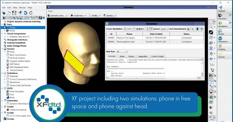
Integration with Full-Wave Simulation
A key highlight of the schematic editor is its integration with full-wave simulation technologies. This seamless integration plays a pivotal role in bridging the gap between the theoretical schematic-based results and the practical, observable outcomes derived from full-wave simulations. Such outcomes include detailed far-zone radiation patterns and intricate surface current analyses, which are critical for comprehensive antenna design and evaluation. This feature ensures that users can not only design and simulate with accuracy but also validate their results against real-world parameters, enhancing the reliability and effectiveness of the designs produced using the schematic editor.
- Enhanced accuracy by ensuring that modifications in the schematic phase are precisely mirrored in the full-wave simulations
- Smoother workflow transitions from schematic design to physical realization, reducing potential errors and reworks
- Faster iteration cycles, allowing for rapid testing and refinement of antenna designs
- Direct application of theoretical designs into practical, real-world models
- Improved efficiency in design processes, leading to quicker project completions and higher quality outputs

Conclusion
In conclusion, the schematic editor stands out as a robust tool for engineers looking to streamline the design and optimization of matching networks and corporate feed networks. By integrating advanced features such as design goal setting, optimization, and the ability to consider parasitics and coupling--alongside full-wave simulation integration--XF empowers professionals to achieve precise, efficient design outcomes suitable for a range of applications. As the field of electronic design continues to evolve, tools like the schematic editor will be crucial in navigating the complexities of modern circuit design.