Touchscreen 3x4 Diamond Simulation with XF's Electrostatic Solver
The geometry of this touch screen example is taken from reference [1] and consists of three driving electrodes in the XY plane at z = 0 and four sensing electrodes in the XY plane at z = 254 μm. The structure shown in Figure 1 is generated in XFdtd using the built-in geometry tools. One of the lines is first created using a 2D sheet body, and then the other identical lines are created by copying, pasting, and relocating. Once the geometry has been created, the electrodes are set to have a conductivity of 1x10^4 and the dielectric permittivity for the upper, middle, and lower substrates is set to 7.
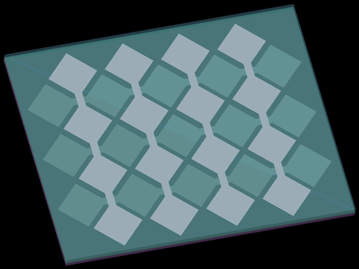
Figure 1: Touch screen geometry with three driving electrodes and four sensing electrodes.
The 7x7 capacitance matrix of the touch screen is simulated using the Electrostatic Solver in XF. The seven electrodes are identified by associating a Static Voltage Point with each of them. The simulated SPICE capacitance matrix for the unloaded case is listed in Table 1. Self capacitance values correspond to values along the diagonal while mutual capacitance values are the off diagonal values.

Table 1: The unloaded SPICE capacitance matrix (fF).
When the screen is loaded, the capacitance will change. In this example, a 1 mm stylus was added and assigned a static voltage of 0V to represent being grounded. The stylus touches the screen above the D2S3 node, as shown in Figure 2. A second electrostatic simulation was run and the loaded SPICE capacitance matrix was computed. The change in capacitance between the loaded and unloaded cases is shown in Tables 2 and 3. In Table 2, the mutual capacitance is highlighted and the location of the stylus can be easily identified in red because it is the only positive change. In Table 3, the self-capacitance values are highlighted. Here, the negative changes indicate the stylus location at electrodes D2 and S3.
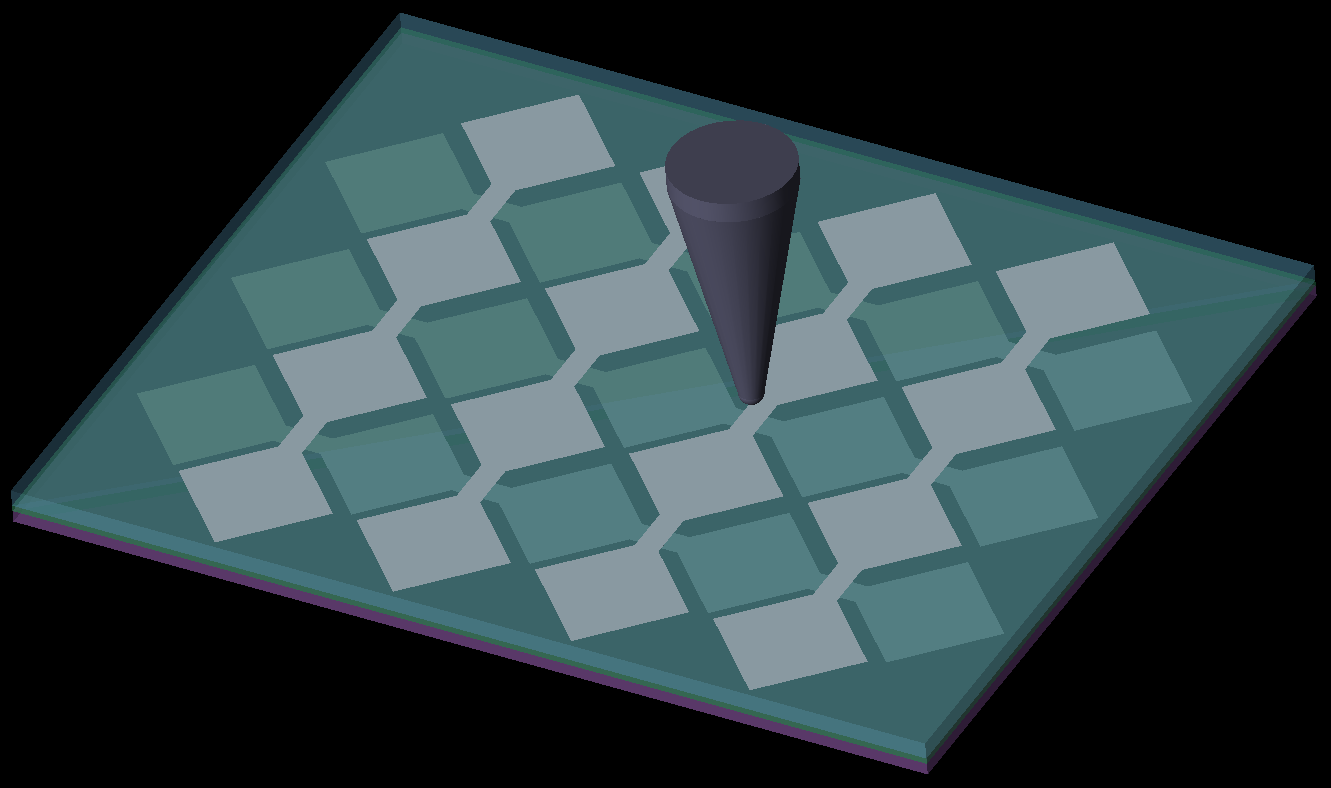
Figure 2: Grounded stylus at the D2S3 node.

Table 2: Change in mutual-capacitance between loaded and unloaded case (fF).

Table 3: Change in self-capacitance between loaded and unloaded case (fF).
The voltage distribution along D2 for is shown in Figure 3. The grounded stylus has a noticeable impact on the voltage and thus causes the change in capacitance.
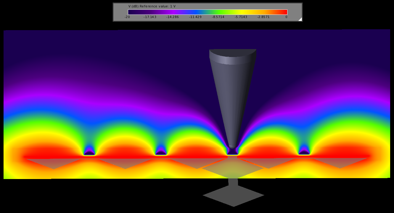
Figure 3: The voltage distribution along D2 when 1V is applied to the electrode.
Reference
-
T. H. Hwang et al., “A Highly Areas-Efficient Controller for Capacitive Touch Screen Panel Systems,” IEEE Transactions on Consumer Electronics, Vol.56, No.2, pp.1115-1122, May 2010.
Request Project Files
Thank you for your interest in this application example. Please complete the form below to download the Touchscreen 3x4 Diamond Simulation with XF's Electrostatic Solver project files.
