Full Wave Simulation: Matching Network Design for GPS / Bluetooth Antenna
A single antenna can be used for GPS and Bluetooth applications if a matching network is properly designed. Once the desired matching network topology is determined using a circuit simulator, full wave simulations are needed to determine the final LC values, because there is parasitic coupling between the antenna and matching network that is not considered by the circuit simulator.
Figure 1 shows the GPS/Bluetooth antenna located at one corner of the mobile device’s PCB. After determining the topology of the matching network, the copper traces are laid out on the PCB (Figure 2). The feed and the shunt inductor are grounded using vias through the substrate. Although the two inductors and single capacitor have been placed, their final values are not known.

Figure 1: GPS/Bluetooth antenna.
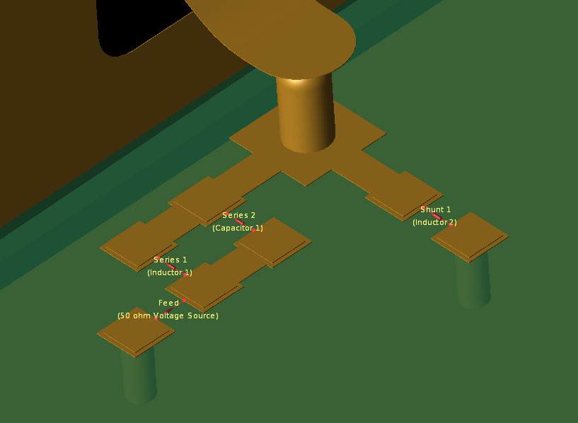
Figure 2: Matching network layout with components in place.
Once all project settings have been defined (material properties, grid, waveform, etc.), XF’s Circuit Element Optimizer is used to characterize the system using XF’s full wave FDTD solver. Then the final component values are determined using the system characterization. Since the FDTD solver is utilized, this process captures and considers all electromagnetic phenomena affecting the matching network’s performance.
As inputs to the optimization, the thresholds for the GPS and Bluetooth bands are provided as goals. The reflection coefficient needs to be below -4 dB and -10 dB for the GPS and Bluetooth bands, respectively. Additionally, the inductor values can range from 0.1 nH to 100 nH, while the capacitor can range from 0.1 pF to 100 pF.
After the optimization has been run, the final component values are provided, as shown in Figure 3. As a verification step, one more FDTD simulation is run by applying the LC component values from the optimization to the project. S11 results are shown in Figure 4. The optimization found component values that met the threshold for the GPS and Bluetooth bands.
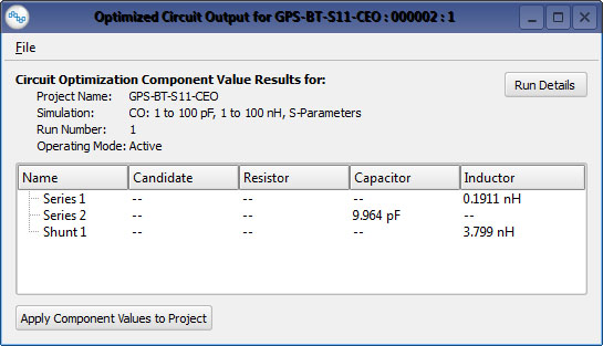
Figure 3: Optimized component values.
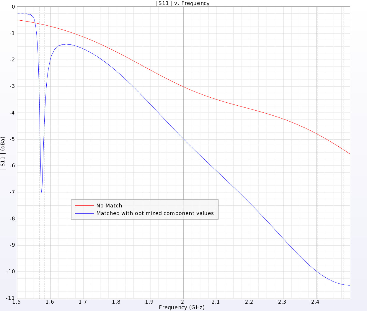
Figure 4: S11 for unmatched and matched antenna.
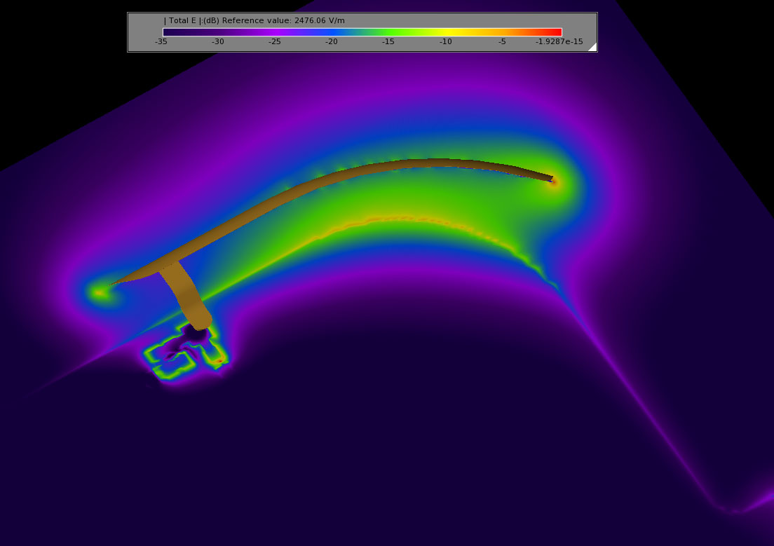
Steady state electric fields through the plane containing the matching network were collected during the final FDTD simulation (Figure 5). The coupling between the antenna and copper traces highlights the importance of considering all electromagnetic effects when determining final LC component values.
